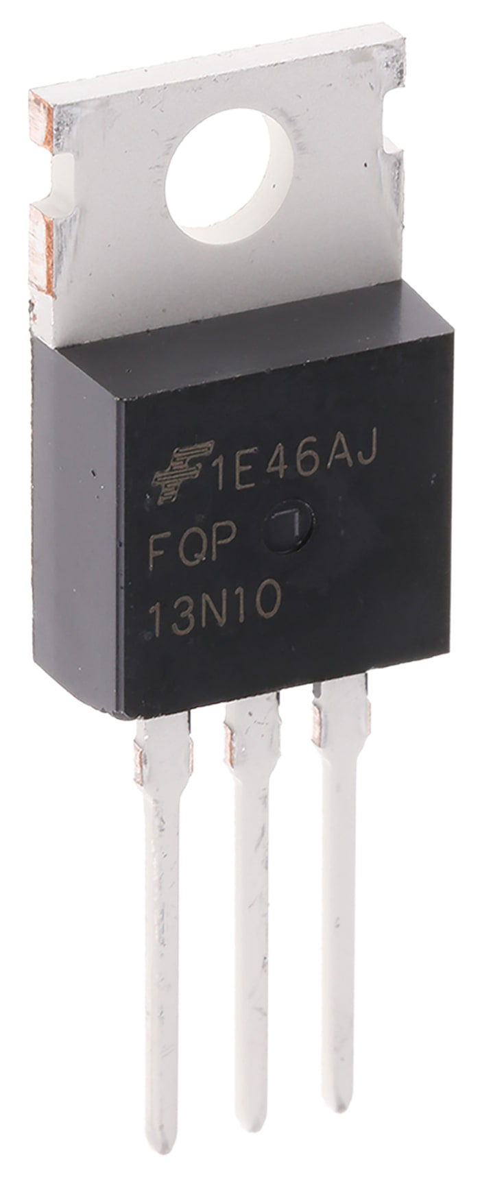
N-Channel MOSFET Transistor, 12.8 A, 100 V, 3-Pin TO-220AB Fairchild FQP13N10L

Technical Document
Specifications
Channel Type
N
Maximum Continuous Drain Current
12.8 A
Maximum Drain Source Voltage
100 V
Package Type
TO-220AB
Mounting Type
Through Hole
Pin Count
3
Maximum Drain Source Resistance
180 mΩ
Channel Mode
Enhancement
Maximum Power Dissipation
65 W
Maximum Gate Source Voltage
-20 V, +20 V
Typical Gate Charge @ Vgs
8.7 nC @ 5 V
Number of Elements per Chip
1
Maximum Operating Temperature
+175 °C
Length
10.1mm
Width
4.7mm
Height
9.4mm
Minimum Operating Temperature
-55 °C
Ideate. Create. Collaborate
JOIN FOR FREE
No hidden fees!


- Download and use our DesignSpark software for your PCB and 3D Mechanical designs
- View and contribute website content and forums
- Download 3D Models, Schematics and Footprints from more than a million products
P.O.A.
Each (In a Pack of 5) (Exc. Vat)
5
P.O.A.
Each (In a Pack of 5) (Exc. Vat)
Stock information temporarily unavailable.
5
Stock information temporarily unavailable.
Ideate. Create. Collaborate
JOIN FOR FREE
No hidden fees!
- Download and use our DesignSpark software for your PCB and 3D Mechanical designs
- View and contribute website content and forums
- Download 3D Models, Schematics and Footprints from more than a million products
Technical Document
Specifications
Channel Type
N
Maximum Continuous Drain Current
12.8 A
Maximum Drain Source Voltage
100 V
Package Type
TO-220AB
Mounting Type
Through Hole
Pin Count
3
Maximum Drain Source Resistance
180 mΩ
Channel Mode
Enhancement
Maximum Power Dissipation
65 W
Maximum Gate Source Voltage
-20 V, +20 V
Typical Gate Charge @ Vgs
8.7 nC @ 5 V
Number of Elements per Chip
1
Maximum Operating Temperature
+175 °C
Length
10.1mm
Width
4.7mm
Height
9.4mm
Minimum Operating Temperature
-55 °C
Ideate. Create. Collaborate
JOIN FOR FREE
No hidden fees!
- Download and use our DesignSpark software for your PCB and 3D Mechanical designs
- View and contribute website content and forums
- Download 3D Models, Schematics and Footprints from more than a million products